Showing posts with label Basic Electronics. Show all posts

Wednesday, July 10, 2013

How to build Mobile Phone Battery Charger Circuit

Description

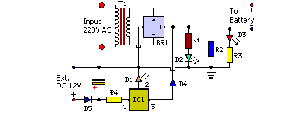
Mobile phone chargers available in the market are quite expensive. The circuit presented here comes as a low-cost alternative to charge mobile telephones/battery packs with a rating of 7.2 volts, such as Nokia 6110/6150.

Circuit diagram:

Circuit diagram:

Parts

  • R1 = 1K
  • R2 = 47R
  • R3 = 10R
  • R4 = 47R
  • C1 = 1000uF-25V
  • D1 = LEDs any color
  • D2 = LEDs any color
  • D3 = LEDs any color
  • D4 = 1N4007
  • D5 = 1N4007
  • IC1 = LM7806
  • T1 = 9VAC Xformer 250mA
  • BR1 = Diode bridge 1A

Circuit Operation:

The 220-240V AC mains supply is down-converted to 9V AC by transformer T1. The transformer output is rectified by BR1 and the positive DC supply is directly connected to the charger’s output contact, while the negative terminal is connected through current limiting resistor R2. D2 works as a power indicator with R1 serving as the current limiter and D3 indicates the charging status. During the charging period, about 3 volts drop occurs across R2, which turns on D3 through R3.
An external DC supply source (for instance, from a vehicle battery) can also be used to energies the charger, where R4, after polarity protection diode D5, limits the input current to a safe value. The 3-terminal positive voltage regulator LM7806 (IC1) provides a constant voltage output of 7.8V DC since D1 connected between the common terminal (pin 2) and ground rail of IC1 raises the output voltage to 7.8V DC. D1 also serves as a power indicator for the external DC supply. After constructing the circuit on a veroboard, enclose it in a suitable cabinet. A small heat sink is recommended for IC1.


Description

Charging of the mobile phone, cellphone battery is a big problem while traveling as power supply source is not generally accessible. If you keep your cellphone switched on continuously, its battery will go flat within five to six hours, making the cellphone useless.
A fully charged battery becomes necessary especially when your distance from the nearest relay station increases. Here’s a simple charger that replenishes the cellphone battery within two to three hours. Basically, the charger is a current-limited voltage source. Generally, cellphone battery packs require 3.6-6V DC and 180-200mA current for charging. These usually contain three NiCd cells, each having 1.2V rating.
Current of 100mA is sufficient for charging the cellphone battery at a slow rate. A 12V battery containing eight pen cells gives sufficient current (1.8A) to charge the battery connected across the output terminals. The circuit also monitors the voltage level of the battery. It automatically cuts off the charging process when its output terminal voltage increases above the predetermined voltage level.

Circuit diagram:

Circuit diagram

Parts:

  • P1 = 20K
  • P2 = 20K
  • R1 = 390R
  • R2 = 680R
  • R3 = 39R-1W
  • R4 = 27K
  • R5 = 47K
  • R6 = 3.3K
  • R7 = 100R-1W
  • C1 = 4.7uF-25V
  • C2 = 0.01uF
  • C3 = 0.001uF
  • D1 = 5.6V-1W Zener
  • D2 = 3mm. Red LED
  • Q1 = SL100
  • S1 = On/Off Switch
  • B1 = 1.5vx8 AA Cells in Series
  • IC1 = NE555 Timer IC

Circuit Operation:

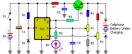
Timer IC NE555 is used to charge and monitor the voltage level in the battery. Control voltage pin 5 of IC1 is provided with a reference voltage of 5.6V by zener diode D1. Threshold pin 6 is supplied with a voltage set by P1 and trigger pin 2 is supplied with a voltage set by P2. When the discharged cellphone battery is connected to the circuit, the voltage given to trigger pin 2 of IC1 is below 1/3Vcc and hence the flip-flop in the IC is switched on to take output pin 3 high. When the battery is fully charged, the output terminal voltage increases the voltage at pin 2 of IC1 above the trigger point threshold.
This switches off the flip-flop and the output goes low to terminate the charging process. Threshold pin 6 of IC1 is referenced at 2/3Vcc set by P1. Transistor Q1 is used to enhance the charging current. Value of R3 is critical in providing the required current for charging. With the given value of 39-ohm the charging current is around 180 mA. The circuit can be constructed on a small general-purpose PCB.
For calibration of cut-off voltage level, use a variable DC power source. Connect the output terminals of the circuit to the variable power supply set at 7V. Adjust P1 in the middle position and slowly adjust P2 until LED (D2) goes off, indicating low output. LED should turn on when the voltage of the variable power supply reduces below 5V. Enclose the circuit in a small plastic case and use suitable connector for connecting to the cellphone battery.

Monday, September 17, 2012

Using a Multimeter

source: http://mechatronics.mech.northwestern.edu/design_ref/tools/multimeter.html
A multimeter is used to make various electrical measurements, such as AC and DC voltage, AC and DC current, and resistance. It is called amultimeter because it combines the functions of a voltmeter, ammeter, and ohmmeter. Multimeters may also have other functions, such as diode and continuity tests. The descriptions and pictures that follow are specific to the Fluke 73 Series III Multimeter, but other multimeters are similar.
Important note: The most common mistake when using a multimeter is not switching the test leads when switching between current sensing and any other type of sensing (voltage, resistance). It is critical that the test leads be in the proper jacks for the measurement you are making.

Safety Information

  • Be sure the test leads and rotary switch are in the correct position for the desired measurement.
  • Never use the meter if the meter or the test leads look damaged.
  • Never measure resistance in a circuit when power is applied.
  • Never touch the probes to a voltage source when a test lead is plugged into the 10 A or 300 mA input jack.
  • To avoid damage or injury, never use the meter on circuits that exceed 4800 watts.
  • Never apply more than the rated voltage between any input jack and earth ground (600 V for the Fluke 73).
  • Be careful when working with voltages above 60 V DC or 30 V AC rms. Such voltages pose a shock hazard.
  • Keep your fingers behind the finger guards on the test probes when making measurements.
  • To avoid false readings, which could lead to possible electric shock or personal injury, replace the battery as soon as the battery indicator appears.

Input Jacks

 
The black lead is always plugged into the common terminal. The red lead is plugged into the 10 A jack when measuring currents greater than 300 mA, the 300 mA jack when measuring currents less than 300 mA, and the remaining jack (V-ohms-diode) for all other measurements. 

Range

 
The meter defaults to autorange when first turned on. You can choose a manual range in V AC, V DC, A AC, and A DC by pressing the button in the middle of the rotary dial. To return to autorange, press the button for one second. 

Automatic Touch Hold Mode

The Touch Hold mode automatically captures and displays stable readings. Press the button in the center of the dial for 2 seconds while turning the meter on. When the meter captures a new input, it beeps and a new reading is displayed. To manually force a new measurement to be held, press the center button. To exit the Touch Hold mode, turn the meter off.Note: stray voltages can produce a new reading.
Warning: To avoid electric shock, do not use the Touch Hold to determine if a circuit with high voltage is dead. The Touch Hold mode will not capture unstable or noisy readings. 


AC and DC Voltage


Resistance

 
Turn off the power and discharge all capacitors. An external voltage across a component will give invalid resistance readings. 

Diode Test


Continuity Test

 
This mode is used to check if two points are electrically connected. It is often used to verify connectors. If continuity exists (resistance less than 210 ohms), the beeper sounds continuously. The meter beeps twice if it is in the Touch Hold mode. 

Current

Warning: To avoid injury, do not attempt a current measurement if the open circuit voltage is above the rated voltage of the meter.To avoid blowing an input fuse, use the 10 A jack until you are sure that the current is less than 300 mA.
Turn off power to the circuit. Break the circuit. (For circuits of more than 10 amps, use a current clamp.) Put the meter in series with the circuit as shown and turn power on.

Sunday, September 16, 2012

JTAG Tutorial


http://www.corelis.com/education/JTAG_Tutorial.htm
JTAG Tutorial

Since its introduction as an industry standard in 1990, boundary-scan (also known as JTAG) has enjoyed growing popularity for board level manufacturing test applications. JTAG has rapidly become the technology of choice for building reliable high technology electronic products with a high degree of testability. Due to the low-cost and IC level access capabilities of JTAG, its use has expanded beyond traditional board test applications into product design and service.

This article provides a brief overview of the JTAG architecture and the new technology trends that make using JTAG essential for dramatically reducing development and production costs, speeding test development through automation, and improving product quality because of increased fault coverage. The article also describes the various uses of JTAG and the tools available today for supporting JTAG technology.

Outline


What is JTAG?
JTAG, as defined by the IEEE Std.-1149.1 standard, is an integrated method for testing interconnects on printed circuit boards (PCBs) that are implemented at the integrated circuit (IC) level. The inability to test highly complex and dense printed circuit boards using traditional in-circuit testers and bed of nail fixtures was already evident in the mid eighties. Due to physical space constraints and loss of physical access to fine pitch components and BGA devices, fixturing cost increased dramatically while fixture reliability decreased at the same time.
A Brief History of JTAG
In the 1980s, the Joint Test Action Group (JTAG) developed a specification for JTAG testing that was standardized in 1990 as the IEEE Std. 1149.1-1990. In 1993 a new revision to the IEEE Std. 1149.1 standard was introduced (titled 1149.1a) and it contained many clarifications, corrections, and enhancements. In 1994, a supplement containing a description of the Boundary-Scan Description Language (BSDL) was added to the standard. Since that time, this standard has been adopted by major electronics companies all over the world. Applications are found in high volume, high-end consumer products, telecommunication products, defense systems, computers, peripherals, and avionics. In fact, due to its economic advantages, some smaller companies that cannot afford expensive in-circuit testers are using JTAG.
The JTAG test architecture provides a means to test interconnects between integrated circuits on a board without using physical test probes. It adds a boundary-scan cell that includes a multiplexer and latches to each pin on the device. Boundary-scan cells in a device can capture data from pin or core logic signals, or force data onto pins. Captured data is serially shifted out and externally compared to the expected results. Forced test data is serially shifted into the boundary-scan cells. All of this is controlled from a serial data path called the scan path or scan chain. Figure 1 depicts the main elements of a JTAG device. By allowing direct access to nets, JTAG eliminates the need for a large number of test vectors, which are normally needed to properly initialize sequential logic. Tens or hundreds of vectors may do the job that had previously required thousands of vectors. Potential benefits realized from the use of JTAG are shorter test times, higher test coverage, increased diagnostic capability and lower capital equipment cost.
Typical JTAG Device
Figure 1 - Typical JTAG Device
The principles of interconnect test using JTAG are illustrated in Figure 2. Figure 2 depicts two JTAG compliant devices, U1 and U2, which are connected with four nets. U1 includes four outputs that are driving the four inputs of U2 with various values. In this case, we assume that the circuit includes two faults:  a short between Nets 2 and 3, and an open on Net 4. We will also assume that a short between two nets behaves as a wired-AND and an open is sensed as logic 1. To detect and isolate the above defects, the tester is shifting into the U1 boundary-scan register the patterns shown in Figure 2 and applying these patterns to the inputs of U2. The inputs values of U2 boundary-scan register are shifted out and compared to the expected results. In this case, the results (marked in red) on Nets 2, 3, and 4 do not match the expected values and, therefore, the tester detects the faults on Nets 2, 3, and 4.
JTAG tool vendors provide various types of stimulus and sophisticated algorithms, not only to detect the failing nets, but also to isolate the faults to specific nets, devices, and pins.
Interconnect test example
Figure 2 - Interconnect Test Example


JTAG Chip Architecture
The IEEE-1149.1 standard defines test logic in an integrated circuit which provides applications to perform:
  • Chain integrity testing
  • Interconnection testing between devices
  • Core logic testing (BIST)
  • In-system programming
  • In-Circuit Emulation
  • Functional testing
JTAG Chip Architecture
JTAG Scan Chain with Multiple Chips
JTAG Test Vectors
JTAG Test Vectors

JTAG TAP InterfaceJTAG TAP Interface

JTAG TAP Interface Signals
Abbreviation Signal Description
TCK Test Clock Synchronizes the internal state machine operations
TMS Test Mode State Sampled at the rising edge of TCK to determine the next state
TDI Test Data In Represents the data shifted into the device's test or programming logic. It is sampled at the rising edge of TCK when the internal state machine is in the correct state.
TDO Test Data Out Represents the data shifted out of the device's test or programming logic and is valid on the falling edge of TCK when the internal state machine is in the correct state
TRST Test Reset An optional pin which, when available, can reset the TAP controller's state machine


Required Test Instructions
Working in conjunction with the TAP controller is an IR (Instruction Register) providing which type of test to perform. The 1149.1 Standard requires that all compliant devices must perform the following three instructions:
  • EXTEST Instruction
    The EXTEST instruction performs a PCB interconnect test, places an IEEE 1149.1 compliant device into an external boundary test mode, and selects the boundary scan register to be connected between TDI and TDO. During EXTEST instruction, the boundary scan cells associated with outputs are preloaded with test patterns to test downstream devices. The input boundary cells are set up to capture the input data for later analysis.
  • SAMPLE/PRELOAD Instruction
    The SAMPLE/PRELOAD instruction allows an IEEE 1149.1 compliant device to remain in its functional mode and selects the boundary scan register to be connected between the TDI and TDO pins. During SAMPLE/PRELOAD instruction, the boundary scan register can be accessed through a data scan operation, to take a sample of the functional data input/output of the device. Test data can also be preloaded into the boundary-scan register prior to loading an EXTEST instruction.
  • BYPASS Instruction
    Using the BYPASS instruction, a device's boundary scan chain can be skipped, allowing the data to pass through the bypass register. This allows efficient testing of a selected device without incurring the overhead of traversing through other devices. The BYPASS instruction allows an IEEE 1149.1 compliant device to remain in a functional mode and selects the bypass register to be connected between the TDI and TDO pins. Serial data is allowed to be transferred through a device from the TDI pin to the TDO pin without affecting the operation of the device.

JTAG Applications
While it is obvious that JTAG based testing can be used in the production phase of a product, new developments and applications of the IEEE-1149.1 standard have enabled the use of JTAG in many other product life cycle phases. Specifically, JTAG technology is now applied to product design, prototype debugging and field service as depicted in Figure 3. This means the cost of the JTAG tools can be amortized over the entire product life cycle, not just the production phase.

Product life cycle support
Figure 3 - Product Life Cycle Support

To facilitate this product life cycle concept, JTAG tool vendors such as Corelis offer an integrated family of software and hardware solutions for all phases of a product’s life-cycle. All of these products are compatible with each other, thus protecting the user’s investment.

Applying JTAG for Product Development
The ongoing marketing drive for reduced product size, such as portable phones and digital cameras, higher functional integration, faster clock rates, and shorter product life-cycle with dramatically faster time-to- market has created new technology trends. These trends include increased device complexity, fine pitch components, such as surface-mount technology (SMT), systems-in-package (SIPs), multi-chip modules (MCMs), ball-grid arrays (BGAs), increased IC pin-count, and smaller PCB traces. These technology advances, in turn, create problems in PCB development:
  • Many boards include components that are assembled on both sides of the board. Most of the through-holes and traces are buried and inaccessible.
  • Loss of physical access to fine pitch components, such as SMTs and BGAs, makes it difficult to probe the pins and distinguish between manufacturing and design problems.
  • Often a prototype board is hurriedly built by a small assembly shop with lower quality control as compared to a production house. A prototype generally will include more assembly defects than a production unit.
  • When the prototype arrives, a test fixture for the ICT is not available and, therefore, manufacturing defects cannot be easily detected and isolated.
  • Small-size products do not have test points, making it difficult or impossible to probe suspected nodes.
  • Many Complex Programmable Logic Devices (CPLDs) and flash memory devices (in BGA packages) are not socketed and are soldered directly to the board.
  • Every time a new processor or a different flash device is selected, the engineer has to learn from scratch how to program the flash memory.
  • When a design includes CPLDs from different vendors, the engineer must use different in-circuit programmers to program the CPLDs.
JTAG technology is the only cost-effective solution that can deal with the above problems. In recent years, the number of devices that include JTAG has grown dramatically. Almost every new microprocessor that is being introduced includes JTAG circuitry for testing and in-circuit emulation. Most of the CPLD and field programmable array (FPGA) manufacturers, such as Altera, Lattice and Xilinx, to mention a few, have incorporated JTAG logic into their components, including additional circuitry that uses the JTAG four-wire interface to program their devices in-system.

As the acceptance of JTAG as the main technology for interconnect testing and in-system programming (ISP) has increased, the various JTAG test and ISP tools have matured as well. The increased number of JTAG components and mature JTAG tools, as well as other factors that will be described later, provide engineers with the following benefits:
  • Easy to implement Design-For- Testability (DFT) rules. A list of basic DFT rules is provided later in this article.
  • Design analysis prior to PCB layout to improve testability.
  • Packaging problems are found prior to PCB layout.
  • Little need for test points.
  • No need for test fixtures.
  • More control over the test process.
  • Quick diagnosis (with high resolution) of interconnection problems without writing any functional test code.
  • Program code in flash devices.
  • Design configuration data placement into CPLDs.
  • JTAG emulation and source-level debugging.

What JTAG Tools are needed?
In the previous section, we listed many of the benefits that a designer enjoys when incorporating boundary-scan in his product development. In this section we describe the tools and design data needed to develop JTAG test procedures and patterns for ISP, followed by a description of how to test and program a board. We use a typical board as an illustration for the various JTAG test functions needed. A block diagram of such a board is depicted in Figure 4.
Typical board with boundary-scan components
Figure 4 - Typical Board with JTAG Components
 
A typical digital board with JTAG devices includes the following main components: 
  • Various JTAG components such as CPLDs, FPGAs, Processors, etc., chained together via the boundary-scan path.
  • Non-JTAG components (clusters).
  • Various types of memory devices.
  • Flash Memory components.
  • Transparent components such as series resistors or buffers. 
Most of the boundary-scan test systems are comprised of two basic elements: Test Program Generation and Test Execution. Generally, a Test Program Generator (TPG) requires the netlist of the Unit Under Test (UUT) and the BSDL files of the JTAG components. The TPG automatically generates test patterns that allow fault detection and isolation for all JTAG testable nets of the PCB. A good TPG can be used to create a thorough test pattern for a wide range of designs. For example, ScanExpress TPG typically achieves net coverage of more than 60%, even though the majority of the PCB designs are not optimized for boundary-scan testing. The TPG also creates test vectors to detect faults on the pins of non-scannable components, such as clusters and memories that are surrounded by scannable devices.

Some TPGs also generate a test coverage report that allows the user to focus on the non-testable nets and determine what additional means are needed to increase the test coverage.

Test programs are generated in seconds. For example, when Corelis ScanExpress TPG™ was used, it took a 3.0 GHz Pentium 4 PC 23 seconds to generate an interconnect test for a UUT with 5,638 nets (with 19,910 pins). This generation time includes netlist and all other input files processing as well as test pattern file generation.

Test execution tools from various vendors provide means for executing JTAG tests and performing in-system programming in a pre-planned specific order, called a test plan. Test vectors files, which have been generated using the TPG, are automatically applied to the UUT and the results are compared to the expected values. In case of a detected fault, the system diagnoses the fault and lists the failures as depicted in Figure 5. Figure 5 shows the main window of the Corelis test execution tool, ScanExpress Runner™. ScanExpress Runner gives the user an overview of all test steps and the results of executed tests. These results are displayed both for individual tests as well as for the total test runs executed. ScanExpress Runner provides the ability to add or delete various test steps from a test plan, or re-arrange the order of the test steps in a plan. Tests can also be enabled or disabled and the test execution can be stopped upon the failure of any particular test.

Different test plans may be constructed for different UUTs. Tests within a test plan may be re-ordered, enabled or disabled, and unlimited different tests can be combined into a test plan. ScanExpress Runner can be used to develop a test sequence or test plan from various independent sub-tests. These sub-tests can then be executed sequentially as many times as specified or continuously if desired. A sub-test can also program CPLDs and flash memories. For ISP, other formats, such as SVF, JAM, and STAPL, are also supported.

To test the board depicted in Figure 4, the user must execute a test plan that consists of various test steps as shown in Figure 5.
ScanExpress Runner Main Window

Figure 5 - ScanExpress Runner Main Window
 
The first and most important test is the scan chain infrastructure integrity test. The scan chain must work correctly prior to proceeding to other tests and ISP. Following a successful test of the scan chain, the user can proceed to testing all the interconnections between the JTAG components. If the interconnect test fails, ScanExpress Runner displays a diagnostic screen that identifies the type of failure (such as stuck-at, Bridge, Open) and lists the failing nets and pins as shown in Figure 6. Once the interconnect test passes, including the testing of transparent components, it makes sense to continue testing the clusters and the memory devices. At this stage, the system is ready for in-system programming, which typically takes more time as compared to testing.
ScanExpress Runner Diagnostics Display
Figure 6 - ScanExpress Runner Diagnostics Display
 
During the design phase of a product, some JTAG vendors will provide design assistance in selecting JTAG-compliant components, work with the developers to ensure that the proper BSDL files are used, and provide advice in designing the product for testability.

Applying JTAG for Production Test
Production testing, utilizing traditional In-Circuit Testers that do not have JTAG features installed, experience similar problems that the product developer had and more: 
  • Loss of physical access to fine pitch components, such as SMTs and BGAs, reduces bed-of-nails ICT fault isolation.
  • Development of test fixtures for ICTs becomes longer and more expensive.
  • Development of test procedures for ICTs becomes longer and more expensive due to more complex ICs.
  • Designers are forced to bring out a large number of test points, which is in direct conflict with the goal to miniaturize the design.
  • In-system programming is inherently slow, inefficient, and expensive if done with an ICT.
  • Assembling boards with BGAs is difficult and subject to numerous defects, such as solder smearing.

JTAG Embedded Functional Test
Recently, a test methodology has been developed which combines the ease-of-use and low cost of boundary-scan with the coverage and security of traditional functional testing. This new technique, called JTAG Emulation Test (JET), lets engineers automatically develop PCB functional test that can be run at full speed., If the PCB has an on-board processor with a JTAG port (common, even if the processor doesn’t support boundary-scan), JET and boundary-scan tests can be executed as part of the same test plan to provide extended fault coverage to further complement or replace ICT testing.

Corelis ScanExpress JET™ provides JTAG embedded test for a wide range of processors. For more information about this technology and product, visit the ScanExpress JET product page.

Production Test Flow
Figure 7 shows different production flow configurations. The diagram shows two typical ways that JTAG is deployed:
  • As a stand-alone application at a separate test station or test bench to test all the interconnects and perform ISP of on-board flash and other memories. JTAG embedded functional test (JET) may be integrated with boundary-scan.
  • Integrated into the ICT system, where the JTAG control hardware is embedded in the ICT system and the boundary-scan (and possibly JET) software is a module called from the ICT software system.
Typical Production Flow Configurations
Figure 7 - Typical Production Flow Configurations

In the first two cases, the test flow is sometimes augmented with a separate ICT stage after the JTAG-based testing is completed, although it is becoming more common for ICT to be skipped altogether or at least to be limited to analog or special purpose functional testing.

The following are major benefits in using JTAG test and in-system programming in production:
  • No need for test fixtures.
  • Integrates product development, production test, and device programming in one tool/system.
  • Engineering test and programming data is reused in Production.
  • Fast test procedure development.
  • Preproduction testing can start the next day when prototype is released to production.
  • Dramatically reduces inventory management – no pre-programmed parts eliminates device handling and ESD damage.
  • Eliminates or reduces ICT usage time – programming and screening.
Production test is an obvious area in which the use of boundary-scan yields tremendous returns. Automatic test program generation and fault diagnostics using JTAG software products and the lack of expensive fixturing requirements can make the entire test process very economical. For products that contain edge connectors and digital interfaces that are not visible from the boundary-scan chain, JTAG vendors offer a family of boundary-scan controllable I/Os that provide a low cost alternative to expensive digital pin electronics.

Field Service and Installation
The role of JTAG does not end when a product ships. Periodic software and hardware updates can be performed remotely using the boundary-scan chain as a non-intrusive access mechanism. This allows flash updates and reprogramming of programmable logic, for example. Service centers that normally would not want to invest in special equipment to support a product now have an option of using a standard PC or laptop for JTAG testing. A simple PC-based JTAG controller can be used for all of the above tasks and also double as a fault diagnostic system, using the same test vectors that were developed during the design and production phase. This concept can be taken one step further by allowing an embedded processor access to the boundary-scan chain. This allows diagnostics and fault isolation to be performed by the embedded processor. The same diagnostic routines can be run as part of a power-on self-test procedure.

JTAG Design-for-Test Basic Considerations
As mentioned earlier in this article, the design for JTAG test guidelines are simple to understand and follow compared to other traditional test requirements. It is important to remember that JTAG testing is most successful when the design and test engineering teams work together to ensure that testability is “designed in” from the start. The boundary-scan chain is the most critical part of JTAG implementations. When that is properly implemented, improved testability inevitably follows.

Below is a list of basic guidelines to observe when designing a JTAG-testable board:
  • If there are programmable components in a chain, such as FPGAs, CPLDs, etc., group them together in the chain order and place the group at either end of the chain. It is recommended that you provide access to Test Data In (TDI) and Test Data Out (TDO) signals where the programmable group connects to the non-programmable devices.
  • All parts in the boundary-scan chain should have 1149.1-compliant test access ports (TAPs).
  • Use simple buffering for the Test Clock (TCK) and Test Mode Select (TMS) signals to simplify test considerations for the boundary-scan TAP. The TAP signals should be buffered to prevent clocking and drive problems.
  • Group similar device families and have a single level converter interface between them, TCK, TMS, TDI, TDO, and system pins.
  • TCK should be properly routed to prevent skew and noise problems.
  • Use the standard JTAG connector on your board as depicted in Corelis documentation.
  • Ensure that BSDL files are available for each JTAG component that is used on your board and that the files are validated.
Design for interconnect testing requires board-level system understanding to ensure higher test coverage and elimination of signal level conflicts.
  • Determine which JTAG components are on the board. Change as many non-JTAG components to IEEE 1149.1-compliant devices as possible in order to maximize test coverage.
  • Check non-JTAG devices on the board and design disabling methods for the outputs of those devices in order to prevent signal level conflicts. Connect the enable pins of the conflicting devices to JTAG controllable outputs. Corelis tools will keep the enable/disable outputs at a fixed disabling value during the entire test.
  • Ensure that your memory devices are surrounded by JTAG components. This will allow you to use a test program generator, such as ScanExpress TPG, to test the interconnects of the memory devices.
  • Check the access to the non-boundary-scan clusters. Make sure that the clusters are surrounded by JTAG components. By surrounding the non-boundary-scan clusters with JTAG devices, the clusters can then be tested using a JTAG test tool.
  • If your design includes transparent components, such as series resistors or non-inverting buffers, your test coverage can be increased by testing through these components using ScanExpress TPG.
  • Connect all I/Os to JTAG controllable devices. This will enable the use of JTAG, digital I/O module, such as the ScanIO-300LV, to test all your I/O pins, thus increasing test coverage.

Summary
JTAG is a widely practiced test methodology that is reducing costs, speeding development, and improving product quality for electronics manufacturers around the world. By relying on an industry standard, IEEE 1149.1, it is relatively quick, easy, and inexpensive to deploy a highly effective test procedure. Indeed, for many of today’s PCBs, there is little alternative because of limited access to board-level circuitry. This paper highlights just some of the potential applications of the JTAG standard in various stages of the product life cycle, each contributing to the overall effect of significantly reduced product development and support costs.

References
The IEEE Std 1149.1-1990 - Test Access Port and JTAG Architecture, and the Std 1149.1-1994b - Supplement to IEEE Std 1149.1-1990, are available from the IEEE Inc., 345 East 47th Street, New York, NY 10017, USA, 1-800-678-IEEE (USA), 1-908-981-9667 (Outside of USA). You can also obtain a copy of the IEEE 1149.1 standard from http://www.ieee.com/

Wednesday, September 5, 2012

Basic Electronics

source-http://www.clear.rice.edu/elec201/Book/basic_elec.html
The goal of this chapter is to provide some basic information about electronic circuits. We make the assumption that you have no prior knowledge of electronics, electricity, or circuits, and start from the basics. This is an unconventional approach, so it may be interesting, or at least amusing, even if you do have some experience. So, the first question is ``What is an electronic circuit?'' A circuit is a structure that directs and controls electric currents, presumably to perform some useful function. The very name "circuit" implies that the structure is closed, something like a loop. That is all very well, but this answer immediately raises a new question: "What is an electric current?" Again, the name "current" indicates that it refers to some type of flow, and in this case we mean a flow of electric charge, which is usually just called charge because electric charge is really the only kind there is. Finally we come to the basic question:

What is Charge?

 
No one knows what charge really is anymore than anyone knows what gravity is. Both are models, constructions, fabrications if you like, to describe and represent something that can be measured in the real world, specifically a force. Gravity is the name for a force between masses that we can feel and measure. Early workers observed that bodies in "certain electrical condition" also exerted forces on one another that they could measure, and they invented charge to explain their observations. Amazingly, only three simple postulates or assumptions, plus some experimental observations, are necessary to explain all electrical phenomena. Everything: currents, electronics, radio waves, and light. Not many things are so simple, so it is worth stating the three postulates clearly.

Charge exists.   

We just invent the name to represent the source of the physical force that can be observed. The assumption is that the more charge something has, the more force will be exerted. Charge is measured in units of Coulombs, abbreviated C. The unit was named to honor Charles Augustin Coulomb (1736-1806) the French aristocrat and engineer who first measured the force between charged objects using a sensitive torsion balance he invented. Coulomb lived in a time of political unrest and new ideas, the age of Voltaire and Rousseau. Fortunately, Coulomb completed most of his work before the revolution and prudently left Paris with the storming of the Bastille.

Charge comes in two styles.

We call the two styles positive charge, + , and (you guessed it) negative charge, - . Charge also comes in lumps of 1.6 �10-19C , which is about two ten-million-trillionths of a Coulomb. The  discrete nature of charge is not important for this discussion, but it does serve to indicate that a Coulomb is a LOT of charge.

Charge is conserved.

You cannot create it and you cannot annihilate it. You can, however, neutralize it. Early workers observed experimentally that if they took equal amounts of positive and negative charge and combined them on some object, then that object neither exerted nor responded to electrical forces; effectively it had zero net charge. This experiment suggests that it might be possible to take uncharged, or neutral, material and to separate somehow the latent positive and negative charges. If you have ever rubbed a balloon on wool to make it stick to the wall, you have separated charges using mechanical action.
Those are the three postulates. Now we will present some of the experimental findings that both led to them and amplify their significance.

Voltage   


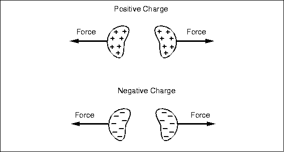
First we return to the basic assumption that forces are the result of charges. Specifically, bodies with opposite charges attract, they exert a force on each other pulling them together. The magnitude of the force is proportional to the product of the charge on each mass. This is just like gravity, where we use the term "mass" to represent the quality of bodies that results in the attractive force that pulls them together (see Fig. 4.1).


Figure 4.1: Opposite charges exert an attractive force on each other, just like two masses attract. External force is required to hold them apart, and work is required to move them farther apart.
\begin{figure}
 
\fbox {\centerline{\psfig{figure=basicelec/opp-charge.I}}}\end{figure}

Electrical force, like gravity, also depends inversely on the distance squared between the two bodies; short separation means big forces. Thus it takes an opposing force to keep two charges of opposite sign apart, just like it takes force to keep an apple from falling to earth. It also takes work and the expenditure of energy to pull positive and negative charges apart, just like it takes work to raise a big mass against gravity, or to stretch a spring. This stored or potential energy can be recovered and put to work to do some useful task. A falling mass can raise a bucket of water; a retracting spring can pull a door shut or run a clock. It requires some imagination to devise ways one might hook on to charges of opposite sign to get some useful work done, but it should be possible.
The potential that separated opposite charges have for doing work if they are released to fly together is called voltage, measured in units of volts (V). (Sadly, the unit volt is not named for Voltaire, but rather for Volta, an Italian scientist.) The greater the amount of charge and the greater the physical separation, the greater the voltage or stored energy. The greater the voltage, the greater the force that is driving the charges together. Voltage is always measured between two points, in this case, the positive and negative charges. If you want to compare the voltage of several charged bodies, the relative force driving the various charges, it makes sense to keep one point constant for the measurements. Traditionally, that common point is called "ground."
Early workers, like Coulomb, also observed that two bodies with charges of the same type, either both positive or both negative, repelled each other (Fig. 4.2). They experience a force pushing


Figure 4.2: Like charges exert a repulsive force on each other. External force is required to hold them together, and work is required to push them closer.
\begin{figure}

\fbox {\centerline{\psfig{figure=basicelec/like-charge.I}}}\end{figure}

them apart, and an opposing force is necessary to hold them together, like holding a compressed spring. Work can potentially be done by letting the charges fly apart, just like releasing the spring. Our analogy with gravity must end here: no one has observed negative mass, negative gravity, or uncharged bodies flying apart unaided. Too bad, it would be a great way to launch a space probe. The voltage between two separated like charges is negative; they have already done their work by running apart, and it will take external energy and work to force them back together.
So how do you tell if a particular bunch of charge is positive or negative? You can't in isolation. Even with two charges, you can only tell if they are the same (they repel) or opposite (they attract). The names are relative; someone has to define which one is "positive." Similarly, the voltage between two points A and B , VAB , is relative. If VAB is positive you know the two points are oppositely charged, but you cannot tell if point A has positive charge and point B negative, or visa versa. However, if you make a second measurement between A and another point C , you can at least tell if B and C have the same charge by the relative sign of the two voltages, VAB and VAC to your common point A . You can even determine the voltage between B and C without measuring it: VBC = VAC - VAB . This is the advantage of defining a common point, like A , as ground and making all voltage measurements with respect to it. If one further defines the charge at point A to be negative charge, then a positive VAB means point B is positively charged, by definition. The names and the signs are all relative, and sometimes confusing if one forgets what the reference or ground point is.


Current   

Charge is mobile and can flow freely in certain materials, called conductors. Metals and a few other elements and compounds are conductors. Materials that charge cannot flow through are called insulators. Air, glass, most plastics, and rubber are insulators, for example. And then there are some materials called semiconductors, that, historically, seemed to be good conductors sometimes but much less so other times. Silicon and germanium are two such materials. Today, we know that the difference in electrical behavior of different samples of these materials is due to extremely small amounts of impurities of different kinds, which could not be measured earlier. This recognition, and the ability to precisely control the "impurities" has led to the massive semiconductor electronics industry and the near-magical devices it produces, including those on your RoboBoard. We will discuss semiconductor devices later; now let us return to conductors and charges.
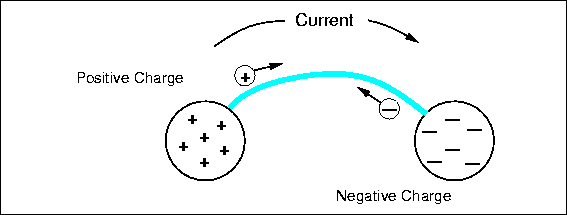
Imagine two oppositely charged bodies, say metal spheres, that are being held apart, as in Fig. 4.3.


Figure 4.3: Two spheres with opposite charges are connected by a conductor, allowing charge to flow.
\begin{figure}
 
\fbox {\centerline{\psfig{figure=basicelec/current.I}}}\end{figure}

There is a force between them, the potential for work, and thus a voltage. Now we connect a conductor between them, a metal wire. On the positively charged sphere, positive charges rush along the wire to the other sphere, repelled by the nearby similar charges and attracted to the distant opposite charges. The same thing occurs on the other sphere and negative charge flows out on the wire. Positive and negative charges combine to neutralize each other, and the flow continues until there are no charge differences between any points of the entire connected system. There may be a net residual charge if the amounts of original positive and negative charge were not equal, but that charge will be distributed evenly so all the forces are balanced. If they were not, more charge would flow. The charge flow is driven by voltage or potential differences. After things have quieted down, there is no voltage difference between any two points of the system and no potential for work. All the work has been done by the moving charges heating up the wire.
The flow of charge is called electrical current. Current is measured in amperes (a), amps for short (named after another French scientist who worked mostly with magnetic effects). An ampere is defined as a flow of one Coulomb of charge in one second past some point. While a Coulomb is a lot of charge to have in one place, an ampere is a common amount of current; about one ampere flows through a 100 watt incandescent light bulb, and a stove burner or a large motor would require ten or more amperes. On the other hand low power digital circuits use only a fraction of an ampere, and so we often use units of 1/1000 of an ampere, a milliamp, abbreviated as ma, and even 1/1000 of a milliamp, or a microamp, �a . The currents on the RoboBoard are generally in the milliamp range, except for the motors, which can require a full ampere under heavy load. Current has a direction, and we define a positive current from point A to B as the flow of positive charges in the same direction. Negative charges can flow as well, in fact, most current is actually the result of negative charges moving. Negative charges flowing from A to B would be a negative current, but, and here is the tricky part, negative charges flowing from B to A would represent a positive current from A to B . The net effect is the same: positive charges flowing to neutralize negative charge or negative charges flowing to neutralize positive charge; in both cases the voltage is reduced and by the same amount.

Batteries   

Charges can be separated by several means to produce a voltage. A battery uses a chemical reaction to produce energy and separate opposite sign charges onto its two terminals. As the charge is drawn off by an external circuit, doing work and finally returning to the opposite terminal, more chemicals in the battery react to restore the charge difference and the voltage. The particular type of chemical reaction used determines the voltage of the battery, but for most commercial batteries the voltage is about 1.5 V per chemical section or cell. Batteries with higher voltages really contain multiple cells inside connected together in series. Now you know why there are 3 V, 6 V, 9 V, and 12 V batteries, but no 4 or 7 V batteries. The current a battery can supply depends on the speed of the chemical reaction supplying charge, which in turn often depends on the physical size of the cell and the surface area of the electrodes. The size of a battery also limits the amount of chemical reactants stored. During use, the chemical reactants are depleted and eventually the voltage drops and the current stops. Even with no current flow, the chemical reaction proceeds at a very slow rate (and there is some internal current flow), so a battery has a finite storage or shelf life, about a year or two in most cases. In some types of batteries, like the ones we use for the robot, the chemical reaction is reversible: applying an external voltage and forcing a current through the battery, which requires work, reverses the chemical reaction and restores most, but not all, the chemical reactants. This cycle can be repeated many times. Batteries are specified in terms of their terminal voltage, the maximum current they can deliver, and the total current capacity in ampere-hours.
You should handle batteries carefully, especially the ones we use in this course. Chemicals are a very efficient and compact way of storing energy. Just consider the power of gasoline or explosives, or the fact that you can play soccer for several hours powered only by a slice of cold pizza for breakfast. Never connect the terminals of a battery together with a wire or other good conductor. The battery we use for the RoboBoard is similar to the battery in cars, which uses lead and sulphuric acid as reactants. Such batteries can deliver very large currents through a short circuit, hundreds of  amperes. The large current will heat the wire and possibly burn you; the resulting rapid internal chemical reactions also produce heat and the battery can explode, spreading nasty, reactive chemicals about. Charging these batteries with too large a current can have the same effect. Double check the circuit and instructions before connecting a battery to any circuit. More information on batteries can be found in Chapter 7.

Circuit Elements

Resistors   

  
We need some way to control the flow of current from a voltage source, like a battery, so we do not melt wires and blow up batteries. If you think of current, charge flow, in terms of water flow, a good electrical conductor is like big water pipe. Water mains and fire hoses have their uses, but you do not want to take a drink from one. Rather, we use small pipes, valves, and other devices to limit water flow to practical levels. Resistors do the same for current; they resist the flow of charge; they are poor conductors. The value of a resistor is measured in ohms and represented by the Greek letter capital omega. There are many different ways to make a resistor. Some are just a coil of wire made of a material that is a poor conductor. The most common and inexpensive type is made from powdered carbon and a glue-like binder. Such carbon composition resistors usually have a brown cylindrical body with a wire lead on each end, and colored bands that indicate the value of the resistor. The key to reading these values is given in Chapter 2.
There are other types of resistors in your robot kit. The potentiometer is a variable resistor. When the knob of a potentiometer is turned, a slider moves along the resistance element. Potentiometers generally have three terminals, a common slider terminal, and one that exhibits increasing resistance and one that has decreasing resistance relative to the slider as the  shaft is turned in one direction. The resistance between the two stationary contacts is, of course, fixed, and is the value specified for the potentiometer. The photoresistor or photocell is composed of a light sensitive material. When the photocell is exposed to more light, the resistance decreases. This type of resistor makes an excellent light sensor.

Ohm's Law

Ohm's law describes the relationship between voltage, V , which is trying to force charge to flow, resistance, R , which is resisting that flow, and the actual resulting current I . The relationship is simple and very basic: \begin{displaymath}
V = I R \quad{\rm or}\quad I = {V \over R} \end{displaymath}.   Thus large voltages and/or low resistances produce large currents. Large resistors limit current to low values. Almost every circuit is more complicated than just a battery and a resistor, so which voltage does the formula refer to? It refers to the voltage across the resistor, the voltage between the two terminal wires. Looked at another way, that voltage is actually produced by the resistor. The resistor is restricting the flow of charge, slowing it down, and this creates a traffic jam on one side, forming an excess of charge with respect to the other side. Any such charge difference or separation results in a voltage between the two points, as explained above. Ohm's law tells us how to calculate that voltage if we know the resistor value and the current flow. This voltage drop is analogous to the drop in water pressure through a small pipe or small nozzle.

Power   

Current flowing through a poor conductor produces heat by an effect similar to mechanical friction. That heat represents energy that comes from the charge traveling across the voltage difference. Remember that separated charges have the potential to do work and provide energy. The work involved in heating a resistor is not very useful, unless we are making a hotplate; rather it is a byproduct of restricting the current flow. Power is measured in units of watts (W), named after James Watt, the Englishman who invented the steam engine, a device for producing lots of useful power. The power that is released into the resistor as heat can be calculated as P=VI , where I is the current flowing through the resistor and V is the voltage across it. Ohm's law relates these two quantities, so we can also calculate the power as \begin{displaymath}
P = {V^2 \over R} \quad {\rm or}\quad P = I^2 R \end{displaymath}The power produced in a resistor raises its temperature and can change its value or destroy it. Most resistors are air-cooled and they are made with different power handling capacity. The most common values are 1/8, 1/4, 1, and 2 watt resistors, and the bigger the wattage rating, the bigger the resistor physically. Some high power applications use special water cooled resistors. Most of the resistors on the RoboBoard are 1/8 watt.

Combinations of Resistors   

 
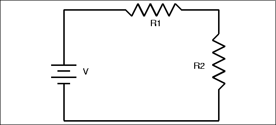
Resistors are often connected together in a circuit, so it is necessary to know how to determine the resistance of a combination of two or more resistors. There are two basic ways in which resistors can be connected: in series and in parallel. A simple series resistance circuit is shown in Figure 4.4.


Figure 4.4: Two Resistors in Series
\begin{figure}

\fbox {\centerline{\psfig{figure=basicelec/resseries.PS}}}\end{figure}

Determining the total resistance for two or more resistors in series is very simple. Total resistance equals the sum of the individual resistances. In this case, RT=R1+R2 . This makes common sense; if you think again in terms of water flow, a series of obstructions in a pipe add up to slow the flow more than any one. The resistance of a series combination is always greater than any of the individual resistors.
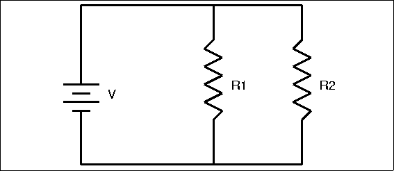
The other method of connecting resistors is shown in Figure 4.5, which shows a simple parallel resistance circuit.


Figure 4.5: Two Resistors in Parallel
\begin{figure}

\fbox {\centerline{\psfig{figure=basicelec/resparallel.PS}}}\end{figure}

Our water pipe analogy indicates that it should be easier for current to flow through this multiplicity of paths, even easier than it would be to flow through any single path. Thus, we expect a parallel combination of resistors to have less resistance than any one of the resistors. Some of the total current will flow through R1 and some will flow through R2, causing an equal voltage drop across each resistor. More current, however, will flow through the path of least resistance. The formula for total resistance in a parallel circuit is more complex than for a series circuit:


RT={1{1R1}+{1R2}...+{1Rn}} (1)
Parallel and series circuits can be combined to make more complex structures, but the resulting complex resistor circuits can be broken down and analyzed in terms of simple series or parallel circuits. Why would you want to use such combinations? There are several reasons; you might use a combination to get a value of resistance that you needed but did not have in a single resistor. Resistors have a maximum voltage rating, so a series of resistors might be used across a high voltage. Also, several low power resistors can be combined to handle higher power. What type of connection would you use?

Capacitors   

  
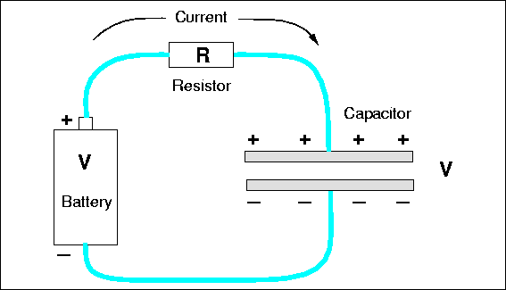
Capacitors are another element used to control the flow of charge in a circuit. The name derives from their capacity to store charge, rather like a small battery. Capacitors consist of two conducting surfaces separated by an insulator; a wire lead is connected to each surface. You can imagine a capacitor as two large metal plates separated by air, although in reality they usually consist of thin metal foils or films separated by plastic film or another solid insulator, and rolled up in a compact package. Consider connecting a capacitor across a battery, as in Fig. 4.6.


Figure 4.6: A simple capacitor connected to a battery through a resistor.
\begin{figure}
 
\fbox {\centerline{\psfig{figure=basicelec/capacitor.I}}}\end{figure}

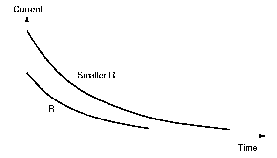
As soon as the connection is made charge flows from the battery terminals, along the wire and onto the plates, positive charge on one plate, negative charge on the other. Why? The like-sign charges on each terminal want to get away from each other. In addition to that repulsion, there is an attraction to the opposite-sign charge on the other nearby plate. Initially the current is large, because in a sense the charges can not tell immediately that the wire does not really go anywhere, that there is no complete circuit of wire. The initial current is limited by the resistance of the wires, or perhaps by a real resistor, as we have shown in Fig. 4.6. But as charge builds up on the plates, charge repulsion resists the flow of more charge and the current is reduced. Eventually, the repulsive force from charge on the plate is strong enough to balance the force from charge on the battery terminal, and all current stops. Figure 4.7 shows how the current might vary with


Figure 4.7: The time dependence of the current in the circuit of Fig. 4.6 for two values of resistance.
\begin{figure}
 
\fbox {\centerline{\psfig{figure=basicelec/decay.I}}}\end{figure}

time for two different values of resistors. For a large resistor, the whole process is slowed because the current is less, but in the end, the same amount of charge must exist on the capacitor plates in both cases. The magnitude of the charge on each plate is equal.
The existence of the separated charges on the plates means there must be a voltage between the plates, and this voltage be equal to the battery voltage when all current stops. After all, since the points are connected by conductors, they should have the same voltage; even if there is a resistor in the circuit, there is no voltage across the resistor if the current is zero, according to Ohm's law. The amount of charge that collects on the plates to produce the voltage is a measure of the value of the capacitor, its capacitance, measured in farads (f). The relationship is C = Q/V , where Q is the charge in Coulombs. Large capacitors have plates with a large area to hold lots of charge, separated by a small distance, which implies a small voltage. A one farad capacitor is extremely large, and generally we deal with microfarads ( �f ), one millionth of a farad, or picofarads (pf), one trillionth (10-12) of a farad.
Consider the   circuit of Fig. 4.6 again. Suppose we cut the wires after all current has stopped flowing. The charge on the plates is now trapped, so there is still a voltage between the terminal wires. The charged capacitor looks somewhat like a battery now. If we connected a resistor across it, current would flow as the positive and negative charges raced to neutralize each other. Unlike a battery, there is no mechanism to replace the charge on the plates removed by the current, so the voltage drops, the current drops, and finally there is no net charge left and no voltage differences anywhere in the circuit. The behavior in time of the current, the charge on the plates, and the voltage looks just like the graph in Fig. 4.7. This curve is an exponential function: exp(-t/RC) . The voltage, current, and charge fall to about 37% of their starting values in a time of R �C seconds, which is called the characteristic time or the time constant of the circuit. The RC time constant is a measure of how fast the circuit can respond to changes in conditions, such as attaching the battery across the uncharged capacitor or attaching a resistor across the charged capacitor. The voltage across a capacitor cannot change immediately; it takes time for the charge to flow, especially if a large resistor is opposing that flow. Thus, capacitors are used in a circuit to damp out rapid changes of voltage.

Combinations of Capacitors   

Like resistors, capacitors can be joined together in two basic ways: parallel and series. It should be obvious from the physical construction of capacitors that connecting two together in parallel results in a bigger capacitance value. A parallel connection results in bigger capacitor plate area, which means they can hold more charge for the same voltage. Thus, the formula for total capacitance in a parallel circuit is:

CT=C1+C2...+Cn , (2)
the same form of equation for resistors in series, which can be confusing unless you think about the physics of what is happening.
The capacitance of a series connection is lower than any capacitor because for a given voltage across the entire group, there will be less charge on each plate. The total capacitance in a series circuit is


CT={1{1C1}+{1C2}...+{1Cn}}. (3)
Again, this is easy to confuse with the formula for parallel resistors, but there is a nice symmetry here.


Inductors   

Inductors are the third and final type of basic circuit component. An inductor is a coil of wire with many windings, often wound around a core made of a magnetic material, like iron. The properties of inductors derive from a different type of force than the one we invented charge to explain: magnetic force rather than electric force. When current flows through a coil (or any wire) it produces a magnetic field in the space outside the wire, and the coil acts just like any natural, permanent magnet, attracting iron and other magnets. If you move a wire through a magnetic field, a current will be generated in the wire and will flow through the associated circuit. It takes energy to move the wire through the field, and that mechanical energy is transformed to electrical energy. This is how an electrical generator works. If the current through a coil is stopped, the magnetic field must also disappear, but it cannot do so immediately. The field represents stored energy and that energy must go somewhere. The field contracts toward the coil, and the effect of the field moving through the wire of the coil is the same as moving a wire through a stationary field: a current is generated in the coil. This induced current acts to keep the current flowing in the coil; the induced current opposes any change, an increase or a decrease, in the current through the inductor. Inductors are used in circuits to smooth the flow of current and prevent any rapid changes.
The current in an inductor is analogous to the voltage across a capacitor. It takes time to change the voltage across a capacitor, and if you try, a large current flows initially. Similarly, it takes time to change the current through an inductor, and if you insist, say by opening a switch, a large voltage will be produced across the inductor as it tries to force current to flow. Such induced voltages can be very large and can damage other circuit components, so it is common to connect some element, like a resistor or even a capacitor across the inductor to provide a current path and absorb the induced voltage. (Often, a diode, which we will discuss later, is used.)
Inductors are measured in henrys (h), another very big unit, so you are more likely to see millihenries, and microhenries. There are almost no inductors on the RoboBoard, but you will be using some indirectly: the motors act like inductors in many ways. In a sense an electric motor is the opposite of an electrical generator. If current flows through a wire that is in a magnetic field (produced either by a permanent magnet or current flowing through a coil), a mechanical force will be generated on the wire. That force can do work. In a motor, the wire that moves through the field and experiences the force is also in the form of a coil of wire, connected mechanically to the shaft of the motor. This coil looks like and acts like an inductor; if you turn off the current (to stop the motor), the coil will still be moving through the magnetic field, and the motor now looks like a generator and can produce a large voltage. The resulting inductive voltage spike can damage components, such as the circuit that controls the motor current. In the past this effect destroyed a lot of motor controller chips and other RoboBoard components. The present board design contains special diodes that will withstand and safely dissipate the induced voltages -- we hope.

Combinations of Inductors

You already know how inductors act in combination because they act just like resistors. Inductance adds in series. This makes physical sense because two coils of wire connected in series just looks like a longer coil. Parallel connection reduces inductance because the current is split between the several coils and the fields in each are thus weaker.

Semiconductor Devices


The Truth About Charge   

Our statements above about charge are not wrong, but they are simple and incomplete. In order to understand how semiconductor devices work one needs a more complete description of the nature of charge in the real world. Charge does not exist independently; it is carried by subatomic particles. For this discussion we will be concerned primarily with electrons, which carry a negative charge of 1.6 � 10-19 C , the minimum amount of charge that can exist in isolation. At least, no one has found any smaller amount than this fundamental quantum of charge.
Electrons are one component of atoms and molecules. Atoms are the building blocks out of which all matter is constructed. Atoms bond with each other to form substances. Substances composed of just one type of atom are called elements. For example, copper, gold and silver are all elements; that is, each of them consists of only one type of atom. More complex substances are made up of more than one atom and are known as compounds. Water, which has both hydrogen and oxygen atoms, is such a compound. The smallest unit of a compound is a molecule. A water molecule, for example, contains two hydrogen atoms and one oxygen atom.
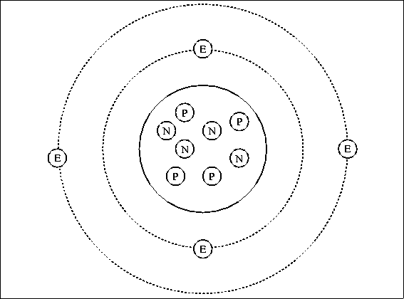
Atoms themselves are made up of even smaller components: protons, neutrons and electrons. Protons and neutrons form the nucleus of an atom, while the electrons orbit the nucleus. Protons carry positive charge and electrons carry negative charge; the magnitude of the charge for both particles is the same, one quantum charge, 1.6 �10-19 C . Neutrons are not charged. Normally, atoms have the same number of protons and electrons and have no net electrical charge.


Figure 4.8: Structure of an Atom
\begin{figure}

\fbox {\centerline{\psfig{figure=basicelec/atomstruct.PS}}}\end{figure}


Electrons that are far from the nucleus are relatively free to move around under the influence of external fields because the force of attraction from the positive charge in the nucleus is weak at large distances. In fact, it takes little force in many cases to completely remove an outer electron from an atom, leaving an ion with a net positive charge. Once free, electrons can move at speeds approaching the speed of light (roughly 670 million miles per hour) through metals, gases and vacuum. They can also become attached to another atom, forming an ion with net negative charge.
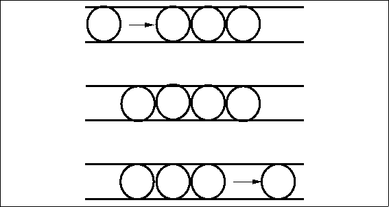
Electric current in metal conductors consists of a flow of free electrons. Because electrons have negative charge, the flow of electrons is in a direction opposite to the positive current. Free electrons traveling through a conductor drift until they hit other electrons attached to atoms. These electrons are then dislodged from their orbits and replaced by the formerly free electrons. The newly freed electrons then start the process anew. At the microscopic level, electron flow through a conductor is not a steady stream, like water flowing from a faucet, but rather a series of short bursts.


Figure 4.9: A Simple Model of Electron Flow
\begin{figure}

\fbox {\centerline{\psfig{figure=basicelec/eflow.PS}}}\end{figure}


Silicon   

 
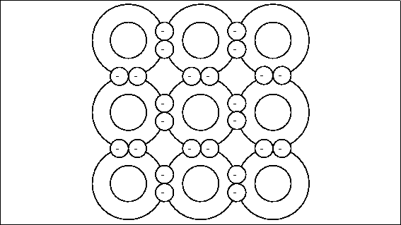
Semiconductor devices are made primarily of silicon (silicon's element symbol is "Si"). Pure silicon forms rigid crystals because of its four valence (outermost) electron structure -- one Si  atom bonds to four other Si atoms forming a very regularly shaped diamond pattern. Figure 4.10 shows part of a silicon crystal structure.


Figure 4.10: A Silicon Crystal Structure
\begin{figure}

\fbox {\centerline{\psfig{figure=basicelec/silicon.PS}}}\end{figure}

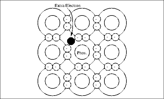
Pure silicon is not a conductor because there are no free electrons; all the electrons are tightly bound to neighboring atoms. To make silicon conducting, producers combine or "dope" pure silicon with very small amounts of other elements like boron or phosphorus. Phosphorus has five outer valence electrons. When three silicon atoms and one phosphorus atom bind together in the basic silicon crystal cell of four atoms, there is an extra electron and a net negative charge. Figure4.11 shows the crystal structure of phosphorus doped silicon.


Figure 4.11: Silicon Doped with Phosphorus
\begin{figure}

\fbox {\centerline{\psfig{figure=basicelec/phosphorus.PS}}}\end{figure}

This type of material is called n-type silicon. The extra electron in the crystal cell is not strongly attached and can be released by normal thermal energy to carry current; the conductivity depends on the amount of phosphorus added to the silicon.
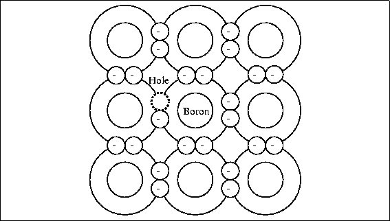
Boron has only three valance electrons. When three silicon atoms and one boron atom bind with each other there is a "hole" where another electron would be if the boron atom were silicon; see Fig. 4.12. This gives the crystal cell a positive net charge (referred to as p-type silicon), and the ability to pick up an electron easily from a neighboring cell.


Figure 4.12: Silicon Doped with Boron
\begin{figure}

\fbox {\centerline{\psfig{figure=basicelec/boron.PS}}}\end{figure}

The resulting migration of electron vacancies or holes acts like a flow of positive charge through the crystal and can support a current. It is sometimes convenient to refer to this current as a flow of positive holes, but in fact the current is really the result of electrons moving in the opposite direction from vacancy to vacancy.

Diodes   

  
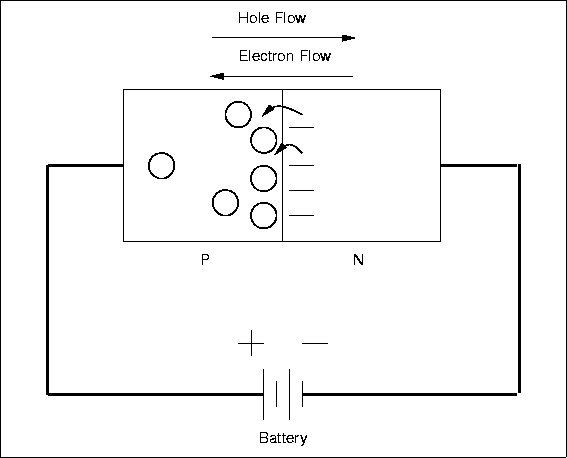
Both p-type and n-type silicon will conduct electricity just like any conductor; however, if a piece of silicon is doped p-type in one section and n-type in an adjacent section, current will flow in only one direction across the junction between the two regions. This device is called a diode and is one of the most basic semiconductor devices.
A diode is called forward biased if it has a positive voltage across it from from the p- to n-type material. In this condition, the diode acts rather like a good conductor, and current can flow, as in Fig. 4.13.


Figure 4.13: A Forward Biased Diode
\begin{figure}

\fbox {\centerline{\psfig{figure=basicelec/fbdiode.PS}}}\end{figure}

There will be a small voltage across the diode, about 0.6 volts for Si, and this voltage will be largely independent of the current, very different from a resistor.
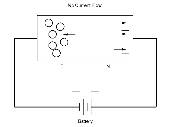
If the polarity of the applied voltage is reversed, then the diode will be reverse biased and will appear nonconducting (Fig. 4.14). Almost no current will flow and there will be a large voltage across the device.


Figure 4.14: A Reverse Biased Diode
\begin{figure}

\fbox {\centerline{\psfig{figure=basicelec/rbdiode.PS}}}\end{figure}

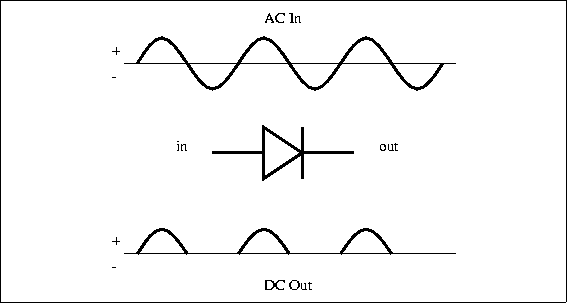
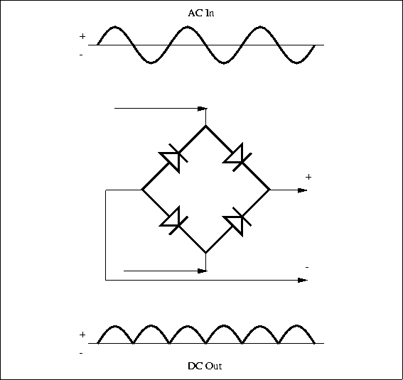
The non-symmetric behavior is due to the detailed properties of the pn-junction. The diode acts like a one-way valve for current and this is a very useful characteristic. One application is to convert alternating current (AC), which changes polarity periodically, into direct current (DC), which always has the same polarity. Normal household power is AC while batteries provide DC, and converting from AC to DC is called rectification. Diodes are used so commonly for this purpose that they are sometimes called rectifiers, although there are other types of rectifying devices. Figure 4.15 shows the input and output current for a simple half-wave


Figure 4.15: A Half-Wave Rectifier
\begin{figure}

\fbox {\centerline{\psfig{figure=basicelec/halfrect.PS}}}\end{figure}

rectifier. The circuits gets its name from the fact that the output is just the positive half of the input waveform. A full-wave rectifier circuit (shown in Figure 4.16) uses four diodes arranged so that both polarities of the input waveform can be used at the output.


Figure 4.16: A Full-Wave Rectifier
\begin{figure}

\fbox {\centerline{\psfig{figure=basicelec/fullrect.PS}}}\end{figure}

The full-wave circuit is more efficient than the half-wave one.